Semiconductor physics
As one of the first five universities in the country to co-found semiconductor physics discipline, Xiamen University has a solid foundation in this field both in teaching and research. Aiming for the international frontier of research and the requirements of national strategy, the university gathered a team of innovative faculties and students focusing on the research of semiconductor materials and the development of semiconductor devices. The university has advanced equipment for growing semiconductor materials and manufacturing semiconductor devices, such as MOCVD, 8" SiC epitaxial system,UHV-CVD, MBE, E-beam, lithography etc. The university's research on Ge, Si, AlGaN, SiC, ZnO and other materials has a strong domestic advantage, contributing significantly to the university's entry into ESI world top 1% in Physics and Material science. Meanwhile, the joint dedication among teaching, research and industry collaboration are promoting the development and boom of the optoelectrical industry in Fujian province of China.
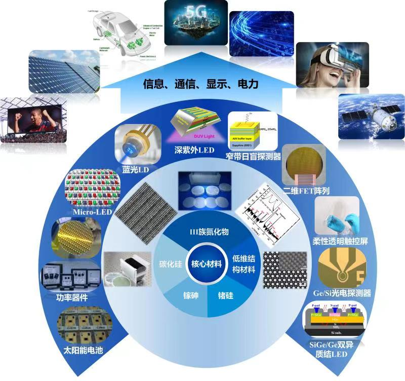
The university's semiconductor discipline has made fruitful achievements by undertaking a number of the nation's missions in research, including national key fundamental, strategical and perspectiveness projects. Areas of research include: high performance micro-LED display; deep ultraviolet (DUV) photoelectric materials and devices; large area SiC epitaxial and power electronic devices; silicon-based optoelectronic materials and devices; oxide semiconductor materials and devices; ultra-wide band gap semiconductor materials and devices; quantum state control and transport of semiconductor; 2D semiconductor materials and devices; energy conversion materials and devices; light-matter interactions in novel semiconductor structures, and so on.
Wide Band-gap Semiconductor Research Group
Introduction: We are interested in: 1、Semiconductor materials and devices; deep ultraviolet LED; solar blind detector; 2、Surface and interface physics, quantum structural materials; 3、Low-dimensional materials, surface plasmon Photonics, new Perovskite Solar Cells; 4、Magnetic Materials and Spintronics, valley Electronics, spintronic devices.
Main Member: KANG Junyong, LI Shuping, CAI Duanjun, WU Zhiming, HUANG Kai, LI Jinchai
Si-based Optoelectronic Material &Device Research Group
Introduction: "Si-based optoelectronic material & device research group consists of five research stuffs and two technique engineers. The group owns valuable semiconductor equipment such as ultra-high-vacuum chemical vapour deposition (UHV-CVD), atomic layer deposition (ALD), magnetic sputtering, and optical/electrical characterization systems. The research scopes of the group include the followed.
1. Si-based optoelectronic integrated circuit is promising for high-speed and low-cost information communication in the next-generation microelectronics. The group-IV materials such as Ge and GeSn are naturally silicon-compatible but still confronted by low light emission efficiency. By introducing bandgap and strain engineering, Ge and GeSn light emission devices were fabricated with high emission efficiency and favored wavelength within the telecommunication wave band. Besides, Si-based Ge photodetectors, with PIN or Schottky structure, were also fabricated. They performed low dark current, high responsibility, and wide band detection covering the whole telecommunication band.
2. Low-temperature Ge/Si heterogeneous wafer bonding
Low-temperature Ge/Si heterogeneous wafer bonding is a promising method which may replace the traditional epitaxy growth in fabrication of the Si-based Ge film and the Ge/Si photoelectric devices. The bonding process helps to overcome the blocking of large lattice mismatch between foreign materials and improve the crystalline quality of the films. With an amorphous or polycrystalline semiconductor interlayer and combined by the Smart CutTM techniques, high-quality Ge/Si heterogeneous wafer and Ge-on-insulator wafer can be fabricated at present in our group.
3. Silicon-based composites for the next generation lithium-ion battery anodes.
Silicon is a promising anode materials owning to its high theoretical capacity and low discharge potential. However, the huge volume expansion of silicon during charging results in mechanical fracture, loss of inter-particle electrical contact, and repeated chemical side reactions with the electrolyte. By study of the lithiation/delithiation dynamic and interfacial characterization, the group made great efforts to synthesize silicon-based anodes with low cost, high electrochemical performance and long cycle.
4. Synthesis, electronic and optoelectronic properties of 2D materials
As Moore's law approaching its physical limit, new materials including 2D transition metal disulfide (TMD) semiconductors are studied to be combined with traditional silicon. We are doing research work on the synthesis of TMDs using ALD and on the fabrication of TMD transistors to research their electronic properties.
5. Resistive random access memory (RRAM) is promising candidate for next-generation high-density information storage technique due to its fast write/read speed, low power, and scalability. We studied the Pt/HfO2/Ti/n-Si structured 1D1R unit cell for RRAM integration and novel RRAM devices based on solid-electrolytes with new working mechanism."
Main Member: LI Cheng, CHEN Songyan, HUANG Wei, LI Jun
 |